 Block Diagram for FIR Filter Block Diagram for FIR Filter
Here is a mathematical model of Nth order
FIR filter. "D" is a flip-flop
, which means a delay element. N is "Tap
Count" and able to be 4 to 380.

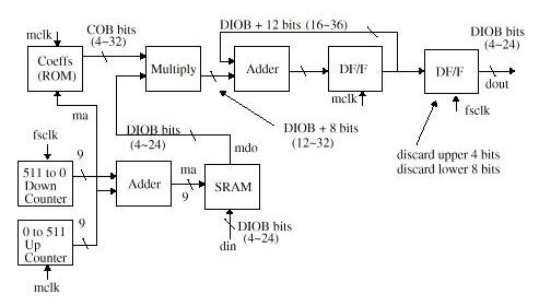
Block diagram of VHDL code is drawn like
following. Data consists of DIOB bits(4 to
24) and is written into RAM. Coefficients
consist of COB bits(4 to 32) and are read
from ROM. We have only one DIOBxCOB multiplier
and it accumulates its output to get filtered
output, which consists of DIOB bits. Note:
SRAM can be huge size and is not good for synthesis. You'd better use a
hard macro cell or external SRAM.
Back
|